

Most of you heard about the word ‘semiconductor‘, but do you know what does it exactly mean? Semiconductors are material in which the forbidden energy gap between the valence band and the conduction band is small or the Fermi energy level is less. In other words, it has a conductivity that is somehow between metals and insulators.
One of the most renowned semiconductors is silicon. Apart from this, germanium, arsenide, and cadmium selenide are other examples of it. To understand the semiconductors, we must know some important terms related to it. Let’s start by knowing them first.
Table of Contents
Meaning of Semiconductors
Semiconductors are elements either man-made or natural, which have a conductivity of electrons between conductors and insulators. The special thing about them is they act as insulators at room temperature and start behaving as conductors as temperature rises. Doping some impurities leads to conduction at room temperature also. The process of adding impurities is doping.
These are the most important part of electronic devices in today’s era. The nature and type of semiconductors depend on the charge carriers inside it, viz, electrons, ions, and holes. You will tell know about the concept of holes further in the article. To understand better about semiconductors, there are some terminologies which you should know. Now let’s start by knowing those terms.
Useful Terminologies
Fermi Energy Level
You have noticed this word in the 1st paragraph, I know some of you have wondered what does it mean. The concept of this energy level is based on Pauli’s exclusion principle which comes under Quantum physics. This principle states, “each allowed energy level can be accumulated by only two electrons with opposite spins”. The Fermi Energy level means that at lower temperatures the available states in an atom will be occupied by two electrons. The probability of electron occupation is given by the Fermi-Dirac Distribution Function. This is given by the following formula:-
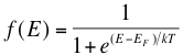
In the above formula, T is temperature, E is the possible energy state, k is Boltzmann’s constant (1.38 x 10⁻²³ J/k), EF is the Fermi Energy level and e is a charge of a single electron. When we observe the equation we can notice the following things:
- With increasing temperature, there is more possibility of finding electrons in higher energy levels.
- If the temperature drops to absolute zero, then f(E) becomes 1, providing that, all electrons are present below the Fermi level.
- More electrons in the conduction band compared to the valance band at higher temperatures.
Work Function
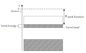
A conducting e– moves freely inside the metal, but it cannot escape the surface of metal without any external force. This barrier for the electron inside the metal is the potential barrier. For an e– to come out from the metal surface, it’s kinetic energy should be equal to or more than the surface potential energy barrier. At absolute zero, the kinetic energy of electrons is equal to the Fermi Energy level.
The work function of a metal is the energy that an electron requires at the Fermi energy level to overcome the potential barrier of the metal. In other words, the work is for the removal of an electron from the metal surface.
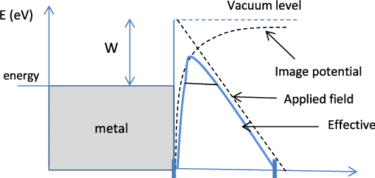
The formula of work function is:- EW = EB-EF = eΦ where Φ is the voltage equivalent of work function, EW is the work function, EB is the height of the surface barrier energy and EF is the maximum value of kinetic energy of the electron. The S.I unit of work function is eV and the typical range is between 1 and 7 eV. Those entities are specified in the picture below for more clarification.
Electron Emission
We can achieve the phenomenon of electron emission by providing external energy in four different ways. These are:-
- Thermionic emission
- Photoelectric emission
- Secondary emission
- Field emission
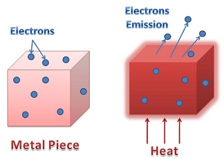
The thermionic emission takes place when you supply additional energy to the electron by heating the metal surface. In the above picture, you can see this representation.
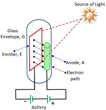
Photoelectric emission occurs when photons of the light strike on the metal surface hence providing extra energy for an electron to escape.
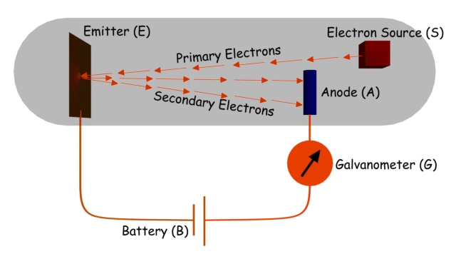
When you supply the energy to the electron by the kinetic energy from outside, it’s Secondary Emission.
Field emission happens when you apply a strong electric field to the metal surface from outside, to accelerate the electron.
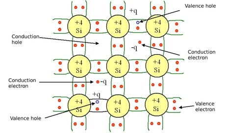
Electron-Hole
The semiconductor has two different types of charge carriers, viz, the electrons and the holes. As most of you know, electrons are the negative charge carriers. On the other hand, the holes are the positive charge carriers.
The concept of holes is a bit confusing. Holes are not separate or physical entities present inside the semiconductors. They are just a result of the movement of electrons.
This means when an electron starts moving from the valance band to the conduction band, a blank space appears. This blank space also known as holes carries the opposite charge of electrons, which is a positive one. We usually indicate the total number of the electron in a semiconductor by n and of the hole by p.
Types of semiconductors
Now you know most of the important words substituted with semiconductors. So, let us start by knowing more about these semiconductors. There are two types of semiconductors, viz, Intrinsic and Extrinsic semiconductors. Now let’s know about them in detail separately.
Intrinsic Semiconductors
They are the Undoped version of semiconductors, also called an i-type semiconductor. Undoped means that this type of semiconductor does not contain any kind of other elements apart from the core semiconductor element.
In other words, the electrical conductivity of a semiconductor entirely determined by the Carriers. These are generated by thermal stations from the balance point to the conduction band then it is an intrinsic semiconductor.
In this type of semiconductor, the number of electrons is equal to the number of holes, i.e., n=p. The pure form of elements like Germanium and Silicon falls under this category. At 0 kelvin or absolute zero intrinsic semiconductors behaves as insulators.
If the semiconductor is kept in room temperatures (20 Celsius) some electrons inside it gain energy. This leads to the movement of electrons from the valance band to the conduction band. This also happens due to the gaining of energy by the electrons and this is called the forbidden energy gap. The forbidden energy gap for Germanium is 0.72 eV and Silicon is 1.1 eV.
Extrinsic Semiconductors
We can say that it is the doped version of Intrinsic semiconductors. In other words, if an Intrinsic Semiconductor doped or mixed with some selected atom impurities, which increases the number of electron or hole. This leads to the formation of Extrinsic Semiconductors. Doping is the process of adding impurities and the impurities added are called dopant.
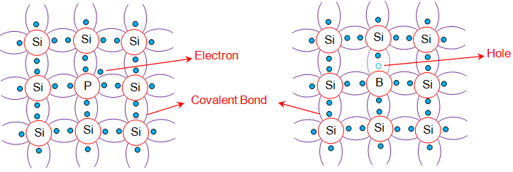
The impurities used as dopants are the elements of groups 3 and 5 of the periodic table. Both groups create a different form of Extrinsic semiconductor. The semiconductor doped with group 3 elements form the p-type and with group 5 elements create the n-type semiconductor. Now let us know about these two different types of semiconductors in detail.
n-Type Semiconductors
This type of semiconductor is formed when a small amount of group 5 elements such as Phosphorus and arsenic are added to germanium or silicon crystal. When the group five elements are added to the crystal, some crystal elements are replaced by the new elements.
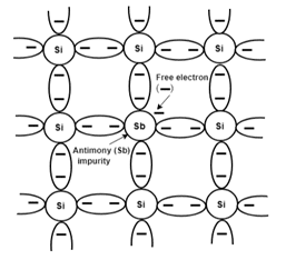
This leads to the generation of free electrons because the crystal atoms only have a valency of 4 but the group 5 elements have a valency of 5. In this, the minority charge carriers are holes and the majority are electrons.
p- Type Semiconductors
This type of semiconductor is formed when a small amount of group 3 elements such as gallium and aluminum are added to germanium or silicon. The same thing as n-type semiconductors happens in p-type also. Group 3 elements replaces some existing atoms in the crystal.
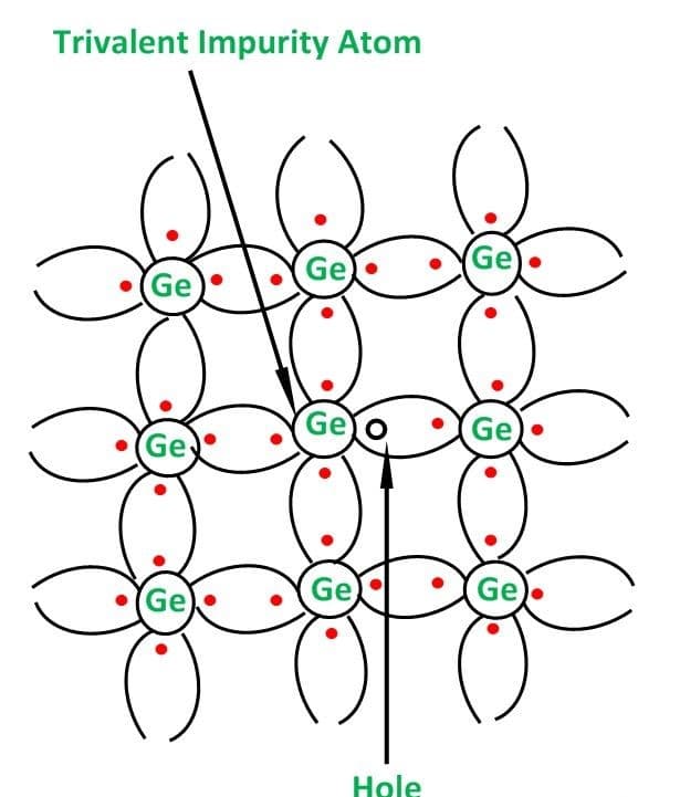
The addition of group 3 elements leads to the generation of a hole as group 3 elements only require 3 electrons in valance shell. In this the majority charge carriers are holes and minority are electrons.
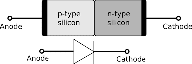
Semiconductor junction diode
This is the most important and basic device formed by using both n and p-type semiconductors. When a single semiconductor doped with n-type elements on one side and p-type on another form diode. The junction where the p and n parts meet is called the depletion layer.
The main function of the device is to make the current flow unidirectional. Junction diodes are of two types, viz, unbiased p-n diode and biased p-n diode. Let us know about them in detail.
The unbiased p-n junction diode
This is the type of p-n junction in which no electrical current flows. The other name for p-n junction diode is zero bias p-n junction. Let us consider a p-n junction in which the n side dominates. Which means, there are more electrons than holes at the junction. Due to the accumulation of more electrons on the n side, they will move towards the p side as it has fewer electrons, and repel force will be less.
It happens because of the Columbus law. This will lead to the movement of electrons and holes on the opposite side. This makes the concentration of electron and holes equal on both sides. We know that when an atom contains the same number of electrons and positive ions it is electrically neutral. This is why the unbiased p-n junction does not have an electrical charge.
When the electrons move towards the opposite side, it increases the positive charge on that side, and the same thing happens with holes. The movement of electrons and holes create a thick layer at the junction. This layer is also known as the depletion layer. The potential generated in the depletion layer is the barrier potential.
The biased p-n junction
This is the p-n junction, in which the flow of electricity is possible. The p-n junction also has two types, viz, the forward biased, and reversed biased.
Forward Biased
A p-n junction becomes forward-biased when we connect the positive side to the p terminal and negative with the n side. In this scenario, the barrier potential is less and more amount of current can flow. This will lead to the formation of covalent bonds between electrons and holes. This process of formation and breaking of covalent bonds make a way for electricity to flow.
When the electrons move to the p side it increases positive charge on n side and the opposite happens on the p side due to the movement of holes towards the n side. Because of the electrical poles on both sides, the positive and negative layers formed at the junction reduces, reducing the barrier potential.
Reversed Biased
This is formed when the n side is connected to the negative terminal and p side to the positive one. When there is no electrical flow, then the standard barrier potential for Germanium is 0.3 volts and 0.7 for Silicon.
Because of the terminal connection the barrier potential increases in reversed biased, leading to the widening of the depletion layer. This widening of the depletion layer happens until the barrier potential becomes equal to the reverse-biased voltage. Because of this, very little flow of electricity takes place in a reversed biased condition.
Semiconductors devices and applications
These are devices that use different properties of electronic components like silicon and germanium. They use solid-state conduction in a vacuum rather than gaseous or liquid states. This is the reason why they are replacing the use of vacuum tubes. They are usually manufactured in circular wafers due to their small size.
Semiconductor devices are famous in industries as their properties can be easily altered. The properties can be changed by doping, temperature variation, and even by heat variations. Other ways are using magnetic and electric fields.
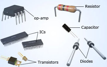
Because of their quick response, they are proven to be made into the best sensors. Devices like diode, capacitors, resistors, sensors, integrated circuits, transistors, operational amplifiers, and many more use semiconductors. There are different categories of semiconductor devices. They are mainly two, three, and four-terminal devices. Here is the list of some devices mentioned below.
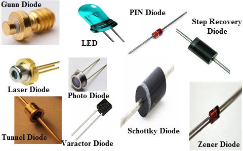
Two terminal:
- Diodes
- Gunn Diode
- IMPATT Diode
- Laser Diode
- Zener Diode
- Schottky Diode
- PIN Diode
- Tunnel Diode
- LED
- Phototransistors
- Photocell
- Solar Cell
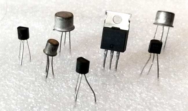
Three Terminal:
- Transistors
- Bipolar
- FET
- Darlington
- IGBT
- Unijuction
- Silicon-controlled Rectifier
- Thyristor
- TRIAC
Four Terminal
- Photo Coupler
- Hall effect sensor
Semiconductor devices advantages and disadvantages
They are basic components required for building logic gates and miniature circuits like microprocessors, MOSFET, transistors, etc. Let us first know what are the advantages of them.
Advantages
- Power is not essential for heating the devices. This happens due to the absence of filament.
- They can be operated immediately after setting up the circuits.
- Do not produce any noise while operating.
- Require low voltage for operation, and are compact because of small size.
- These are shockproof.
- Self-life is very long.
- The cost of buying is very less.
Disadvantages
- Cannot take much power compared to vacuum tubes.
- The noise level is very high in comparison with vacuum tubes.
- They have poor responders for high frequencies.
Conclusion
Semiconductor devices are the backbone of technology industries in today’s era. From small LED’s too big robots, everything requires the use of semiconductors. This is why they play a major role in every aspect of the industries.
Frequently Asked Questions
They are used for making devices like ICs, LED, Resistors, transistors and many more.
Semiconductors are important because of their properties which are very useful in the industrial sector. Their properties can be easily altered by varying temperatures, electrical filed, and by applying other factors. This makes them very useful.
Some examples of semiconductors are Silicon, Germanium, Arsenide and almost all elements in the group VI of the periodic table.
Recent posts
- Protection from Coronavirus: Best Way to Secure Yourself (2020)
- Diffraction of Light: An Amazing phenomenon
- Hydroelectricity: A massive source of electricity (2020)
- Lightsaber colors Mystery: Star Wars Explained
- The Vibrant colors of light: True colors of light
- Virus: Definition, Structure, and Facts regarding virus
- The Big Bang Theory: Origin of the Universe